
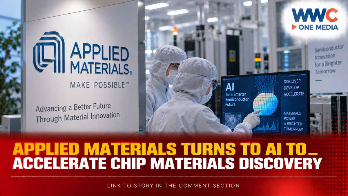
TOKYO — Applied Materials is turning to artificial intelligence to speed up one of the semiconductor industry’s most difficult challenges: developing and optimizing the materials and processes needed to build increasingly advanced chips.
The U.S. semiconductor-equipment giant is expanding the use of AI-powered simulation and materials engineering as chipmakers push toward more sophisticated architectures and increasingly demanding performance requirements.
Applied Materials said in March 2026 that it was accelerating materials simulation for the AI era through a collaboration with NVIDIA, highlighting the growing role of AI in modeling and optimizing semiconductor materials and processes.
The development is significant because advances in chipmaking increasingly depend not only on smaller transistors, but also on discovering and engineering materials that can perform reliably at extremely small scales.
AI could compress years of materials research
Traditional materials development can require extensive simulation, laboratory testing and repeated experimentation.
AI can potentially shorten parts of that cycle by analyzing large amounts of scientific and process data, identifying promising combinations and helping researchers determine which candidates deserve further testing.
For semiconductor manufacturers, even modest improvements in materials or processing can have major implications for chip performance, power consumption, yield and manufacturing costs.
Applied Materials’ approach therefore goes beyond using AI simply to automate factory operations. The company is applying computational tools to the underlying materials-engineering problems involved in semiconductor manufacturing.
Why materials are becoming a bigger chipmaking battleground
The semiconductor industry is approaching physical and engineering limits that make each new generation of chips more difficult to manufacture.
As transistor dimensions shrink and advanced packaging becomes more important, manufacturers must control materials and interfaces with extraordinary precision.
Applied Materials supplies equipment and technologies used in several critical semiconductor manufacturing steps, including deposition, etching, ion implantation, chemical-mechanical polishing, metrology and inspection.
Its position across multiple stages of chip production gives it a broad view of how changes in materials can affect manufacturing.
The company has also been investing heavily in research and development. Its plans for the EPIC Center, a major semiconductor research facility in Silicon Valley, are intended to help accelerate collaboration and development of new chipmaking technologies.
AI is becoming a materials-science tool
Applied Materials is not alone in exploring AI for materials research.
Across the technology and scientific sectors, researchers are using machine learning, computational modeling and increasingly automated laboratory systems to search through enormous numbers of possible materials and predict which candidates could have useful properties.
That matters because the number of possible material combinations can be far too large for researchers to test individually.
AI can help narrow the field.
But it is important to distinguish prediction and simulation from physical discovery and manufacturing validation. A computer-generated candidate still has to be tested experimentally and shown to work reliably in an actual semiconductor process.
Japan’s semiconductor role adds another layer
Japan is a crucial part of the global semiconductor supply chain, particularly in semiconductor materials, chemicals and manufacturing equipment.
Japanese companies supply many of the highly specialized materials and components required by advanced chipmakers, while companies such as Tokyo Electron play major roles in semiconductor manufacturing equipment.
That makes Japan an important market and technology partner as the global industry invests heavily in AI-related semiconductor capacity.
Applied Materials’ push into AI-assisted materials engineering therefore comes as the United States, Japan, Taiwan, South Korea and other economies seek to strengthen their semiconductor ecosystems.
The bigger AI-chip race
The irony is that AI is increasingly being used to improve the very technology needed to run AI.
The explosion of demand for AI computing has pushed chipmakers toward more advanced processors, high-bandwidth memory, advanced packaging and increasingly complex manufacturing technologies.
Applied Materials expects AI-related semiconductor demand to support a prolonged investment cycle, while recent market reporting has highlighted strong demand for its equipment tied to AI computing and advanced semiconductor manufacturing.
If AI can reduce the time required to evaluate new materials and optimize manufacturing processes, it could become an important competitive tool in the next generation of chip development.
Still, the technology remains part of a much larger research pipeline involving scientists, engineers, semiconductor manufacturers and equipment suppliers.
The race is no longer simply to make smaller chips. It is increasingly about finding smarter ways to discover, simulate and manufacture the materials that make those chips possible.




Leave a Reply